What do Phu Le and Dan Jones have in common?
Both of these Cerent engineers worked on the Timing and Control Card (TCC) of the Cerent 454 product. There was not a configuration in which the TCC could be excluded. TCCs had to be equipped in every shelf.
Both of these Cerent engineers worked on the Timing and Control Card (TCC) of the Cerent 454 product. There was not a configuration in which the TCC could be excluded. TCCs had to be equipped in every shelf.
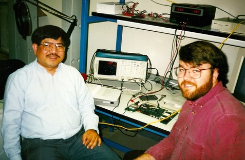
Phu Le (left) working with Dan Jones on TCC, circa 1998. Image courtesy Ajaib Bhadare.
As part of the overall architecture that Ajaib Bhadare and Paul Elliott proposed for this SONET multiplexer, the TCC was assigned the role of main processing center for the ‘454’ shelf to provide system initialization, synchronization, provisioning, alarm reporting, maintenance, and diagnostics for both the shelf in which it was housed and, in part, for the overall network of ‘454s.’ No other vendor had attempted to pack all of these functions into one card before, until Paul architected the TCC in 1997-1998.
As the Cerent engineering team grew in 1998, Dan Jones assumed the role as hardware lead with support from Paul, Dan Kerns wrote the TCC software, and two ASIC engineers produced the TCC ASIC (Phu Le) [1] and the backplane termination ASIC known as BTC or “Betsy” (Martin Roberts). For that matter, Betsy was part of every ‘454’ line card.
This first version of the TCC supported the initial release of the product, the so-called “sweet spot” of the ‘454.’
An enhanced version of the timing and control card, called TCC+, was introduced to support software releases 2.2.1 through 4.1, as the product evolved from the Cerent 454 to the Cisco ONS 15454. The TCC+ was required to support OC-192 capability.
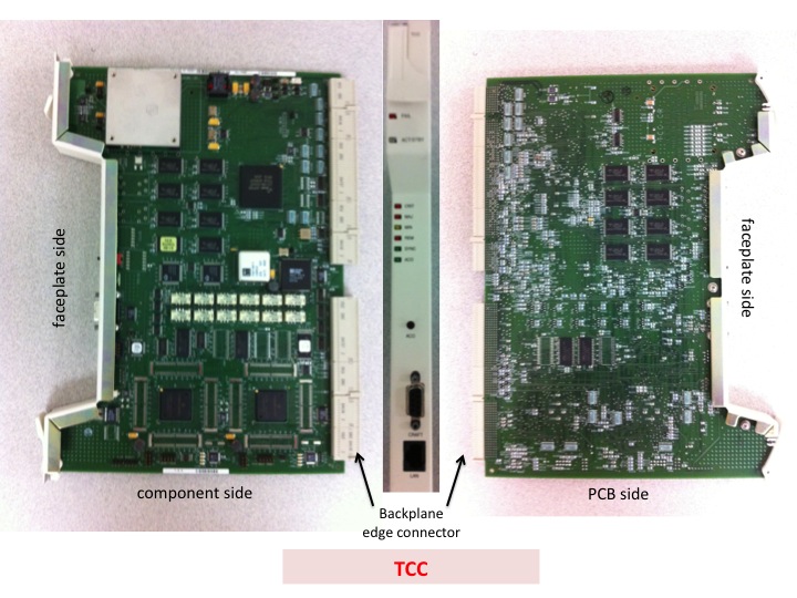
The TCC featured an RJ-45 10BASE-T LAN port and an EIA/TIA-232 DB9 type craft interface for user interfaces. The TL1 craft port ran at 9600 bps. Image courtesy R.K. Koslowsky.
The database for each ‘454’ collection of line cards, the shelf’s unique IP address, and the system software were all stored in the TCC’s nonvolatile memory, which allowed for quick recovery in the event of a power outage or a linecard failure.
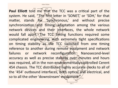
The TCC provided the required system-timing functions for each ‘454’ shelf. It monitored the recovered clocks from each traffic-bearing linecard as well as two DS-1 (BITS) interfaces for frequency accuracy. The TCC had the ability to select its clock source as the system-timing reference: A recovered clock, or a building integrated timing source, or an internal Stratum 3 reference.
The TCC provided the required system-timing functions for each ‘454’ shelf. It monitored the recovered clocks from each traffic-bearing linecard as well as two DS-1 (BITS) interfaces for frequency accuracy. The TCC had the ability to select its clock source as the system-timing reference: A recovered clock, or a building integrated timing source, or an internal Stratum 3 reference.

TCC cards always had to be installed in slots 7 and 11 for redundancy. If the active TCC failed, traffic switched to the standby TCC. The switchover from one TCC to the other conformed to telco protection switching standards of less than 50 ms. It was important to have a backup TCC linecard to avoid a “brain freeze,” not from a Slurpee®, but from a frozen processor.
The TCC symbolized not only the integration of “bleeding edge” technological compactness, but more importantly, the tight collaboration and teamwork among Dan Jones, Phu Le, Martin Roberts, Dan Kerns, and Paul Elliott.
[1] Hui Liu and Paul Elliott told me that the first TCC started out as a field-programmable gate array (FPGA). This implementation was both power-hungry and expensive. Furthermore, FPGAs were generally not rated for extended temperature operating ranges: heatsinks were required to cool them.
Paul outlined the general architecture of the TCC timing section and Dan Jones completed the initial design using FPGAs, since it appeared to be the only game in town. Paul occasionally looking over Dan’s shoulder and made suggestions based on his previous experience. Paul recalls, “We used digital signal processing techniques in this design and had to solve a number of very tricky problems. Dan came up with some extremely clever solutions.”
Hui’s early proposal to turn the FPGA design into an ASIC was turned down by Mike Hatfield for a lack of ASIC resources. Cerent’s ASIC team was busy working on the SXCA and the DS3A to enable the cross-connect (XC) and twelve-port DS-3 linecards, respectively. Besides, using additional foundry resources, which produced an additional non-recurring expense (NRE), made a TCC ASIC cost-prohibitive.
But Hui persevered.
While choosing the DS3A ASIC vendor, Hui happened to talk to Kawasaki representatives, whose operation was based in Japan. Since the little-known Kawasaki (as a telecom components supplier) wanted to enter the red-hot U.S. telecom market in the late 1990s, Hui told them he would award them the DS3A ASIC if they would do the following for Cerent:
1. Shorten the DS3A ASIC schedule by providing more backend resources and giving high priority the DS3A ASIC at their factory, and
2. Spinning the TCCA ASIC at no charge.
Kawasaki agreed and the company delivered both ASICs bug free and ahead of schedule. Mike Hatfield was pleasantly surprised at this fortuitous turn of events. Hui adds, “Phu single-handedly ‘spun’ the TCCA ASIC on the side, while working with Dan on the TCC linecard.”
Paul is proud of Dan and Phu’s collaboration. Paul adds, “Once the timing design had been put through an extensive verification torture-test, it was handed over to Phu for inclusion in the TCC ASIC.”
From a global perspective of the overall ‘454’ design, the TCC established the standardized processor architecture adopted by all other linecards in the system. The TCC project also helped to simplify parts procurement, blaze the trail for board debugging, and define firmware implementation for the ‘454’ product line.
 RSS Feed
